Driving 8250 ACIA without CPU
The goal of the project is to drive an MC8250 ACIA chip and send out “Hello World!” message over a serial connection.
I have a Serial I/O card of RC2014 project. Its circuit diagram looks like this:
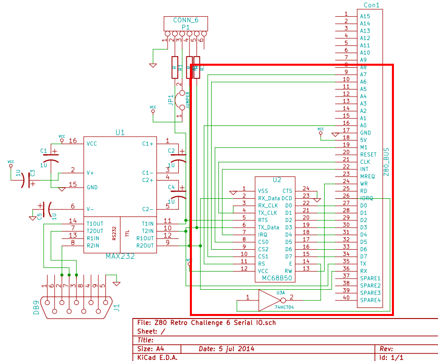
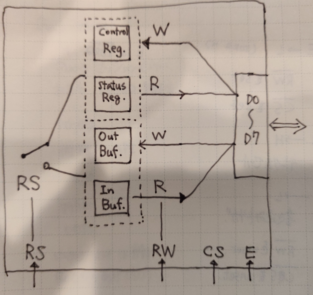
The part that surrounded by the red line is the part we’re interested in. MC68B50 is a faster version of the 6850 chip, and its behavior is practically identical to the original MC6850 in this project. The 6850 chip has two sides of interfaces. One for MPU and another one for serial.
The MPU interface of the 6850 are following pins.
| pin | R/W | Description |
|---|---|---|
| E | W | Enable pin |
| RW | W | Read / write |
| CS0-CS2 | W | Chip Select |
| RS | W | Register Select |
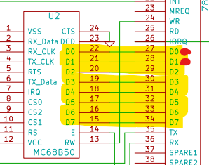
| D0-D7 | R/W | 8-bit data bus |
| IRQ | R | IRQ |
The chip can be communicated via its 4 registers. You can pick which register you want to read or write by setting RS and RW pins. The data you read or write will be on D0-D7 pins. Chip Select (CS) is used to talk to the chip. Enable (E) pin is like a clock for the 8250 chip.
Control sequence
To ask the 8250 to send out message “Hello World!”, we need to following things.
- Initialize the 8250 chip.
- Set up serial port configuration.
- Confirm the configuration was successful.
- Write a character.
- Repeat 4.
In this post, I’m covering the step 1, the initialization of the 8250 chip.
Initialize the 8250 chip
Initialization of the 8250 chip is called “Master Reset” and you can do this by writing a certain value (03h) to the control register.
RS and RW pins
To select the control register, the RS pin should be set to LOW and the RW pin to be LOW (HIGH - READ, LOW - WRITE).
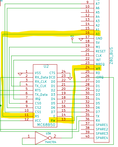
These pins (RS and RW) are connected to RC2014 pins (RS to A0 and RW to WR) respectively.
CS pins
There are three Chip Select (CS0-CS2) pins.
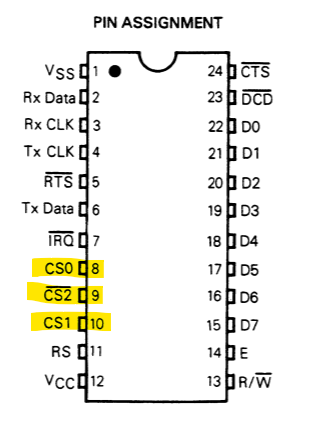
For some reason, 8250’s /CS2 pin is low to active while other two (CS0 and CS1) are high to active. To select the 8250 chip, you need to set CS0 to HIGH, CS1 to HIGH and CS2 to LOW.
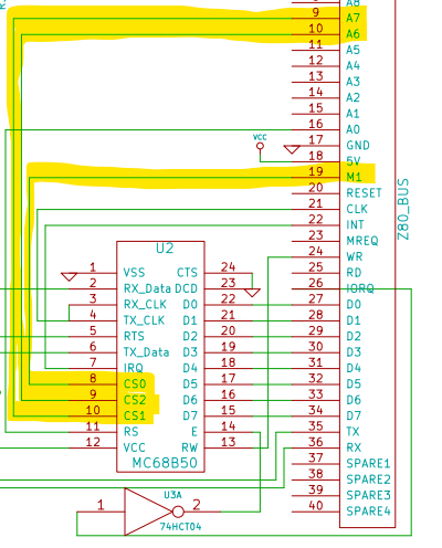
CS0 is connected to M1 pin. Z80’s M1 pin turns on and off during a machine cycle, but for this test, I can just set the M1 pin to HIGH.
CS1 is connected to A7 and /CS2 is connected to A6. RS pin that we reviewed previously is connceted to A0 pin. These will dictate what I/O address should be used to talk to the 8250.
| A7 | A6 | A5 | A4 | A3 | A2 | A1 | A0 |
|---|---|---|---|---|---|---|---|
| 1 | 0 | - | - | - | - | - | 0 |
A5-A1 could be either 0 or 1. The 8250 is selected with 0x80, 0x82, 0x84, 0x86, …, 0x8E, 0x90, 0x92, … 0x9E, 0xA0, … 0xB0, …0xBE, etc. I use 0x80 as the I/O port address.
Data pins
The data is easy. Data pins are connected to corresponding pins. To write 03h, set D0 and D1 to HIGH and D2-D7 to LOW.
E pin
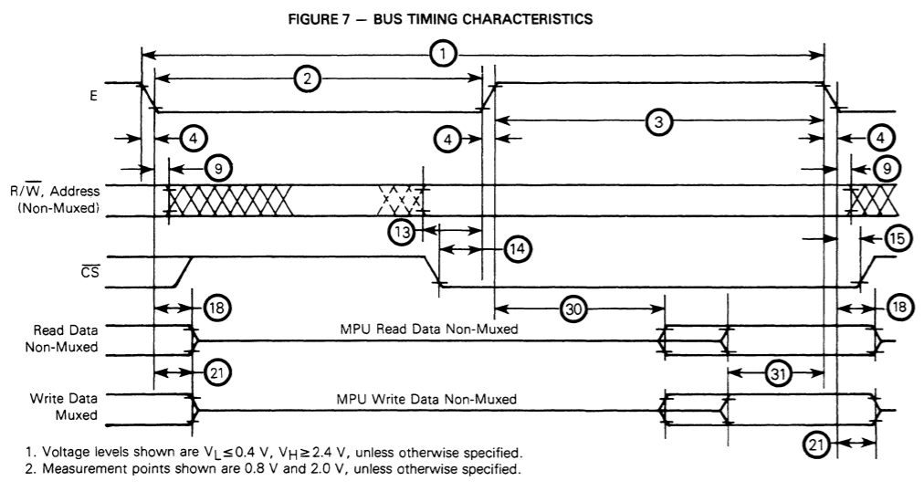
Now, the remaining part is Enable (E) pin, and this was the part I needed some time to understand. The timing chart on the 6850 data sheet was very hard to understand.
I copied the timing chart by hand to understand it.
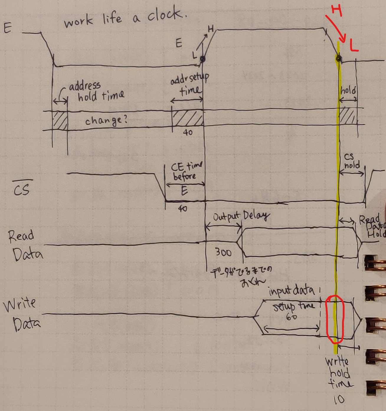
When you are sending data to the 8250, the data on the data bus is read when Enable pin goes from HIGH to LOW (see the red scribbles). We need to set the data certain time before the E pin goes LOW, but the time ins only 60 nano seconds or so, so for this test, I can ignore it.
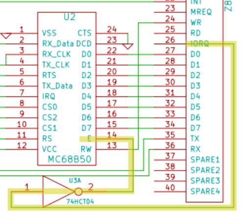
The E pin of the 8250 is connected to IORQ pin of the RC2014 bus. There’s a NOT gate on the line, because Z80 set the IORQ pin LOW when I/O port is used.
Put everything together
With all these, here’s the sequence of actions to reset the 8250:
| On 8255 | On the RC2014 bus |
|---|---|
| Set E pin LOW | IORQ to HIGH |
| Set RW pin LOW(write) | WR pin to HIGH |
| Set RS to LOW | Address bus to 80h |
| Set CS pins active | Address bus to 80h and M1 to HIGH |
| Set E pin to HIGH | IORQ to LOW |
| Set E pin to LOW | IORQ to HIGH => This triggers write |
As the enable (E) pin is like a clock, we move that pin up and down to create a sequence. When you change the E pin value to low at the last step, it triggers a write and master reset action happens soon after that. Unfortunately, I don’t know a way to get the result, but yon can test the status register after sending another configuration command to the 8255 to verify if the initialization was successful.